
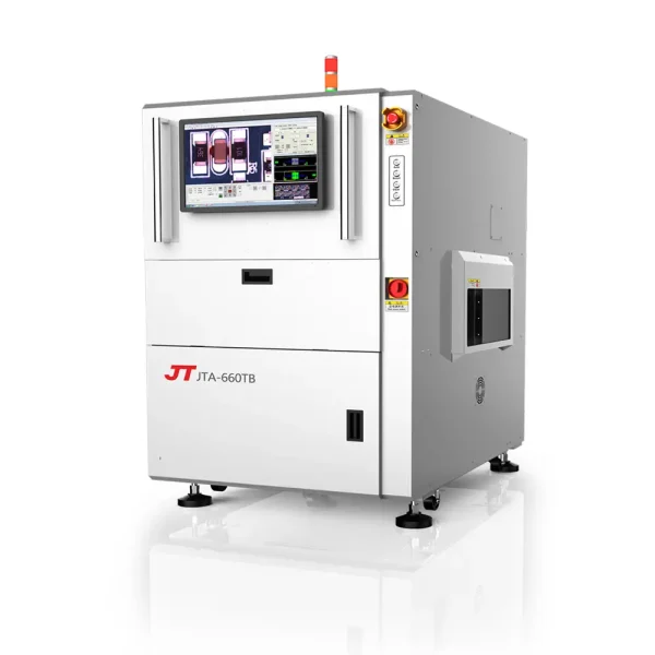
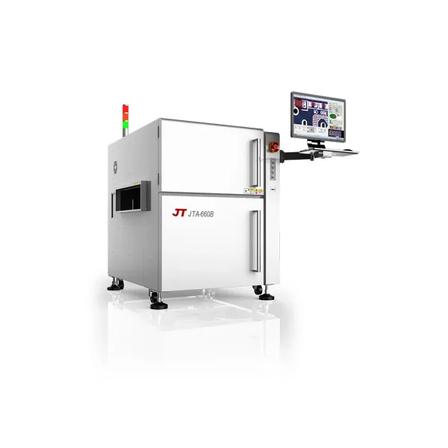
JT AOI JTA-660B
JT JTA-660B inline AOI supports both SMT and DIP PCBA inspection with optional 3D measurement module, ideal for mixed assembly lines with through-hole soldering processes.
JT AOI JTA-660B is a versatile inline Automated Optical Inspection platform compatible with both SMT and DIP assembly processes. It can be upgraded with optional 3D measurement module to deliver height measurement besides standard 2D visual checks, making it suitable for PCBA after wave soldering. The machine adopts high-performance image algorithm to detect DIP-related defects such as missing pins, bent leads, solder voids and bridging, as well as standard SMT component defects. The self-learning algorithm simplifies programming for new PCBA types. It supports large-size PCB and runs stably in high-mix electronics manufacturing. Inspection reports can be exported and integrated with MES for full process quality tracking.
Core Features
Supports SMT and DIP post-wave soldering inspection
Optional 3D measurement module for solder joint height analysis
Powerful algorithm for DIP pin defect detection
Auto-teach programming, fast product changeover
Wide PCB size compatibility
Data export and MES system connection available
Specs (Summary)
Inspection Type: 2D AOI, optional 3D module Application: SMT & DIP wave soldering inspection Min Component: 01005 PCB Thickness: 0.5 ~ 4.0 mm Conveyor: Adjustable width edge clamping conveyor
RELATED PRODUCTS
Inspection & Rework Systems
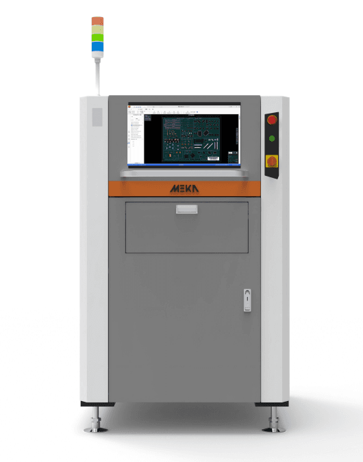
CTW MEKA 2D AOI M2 / M2 Pro / M2 Pro Max
Inspection & Rework Systems
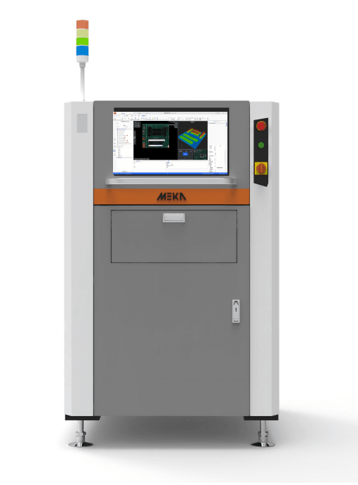
CTW MEKA 3D AOI M3 / M3 Pro / M3 Pro Max / M3 Ultra
Inspection & Rework Systems
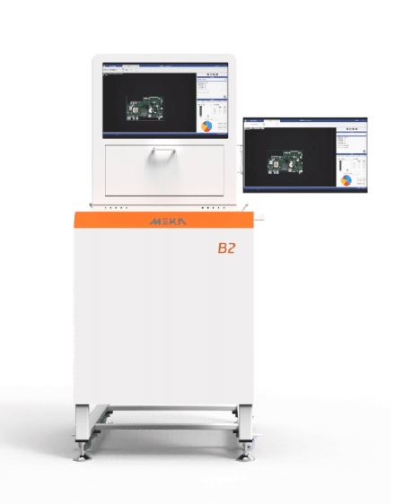
CTW MEKA DIP AOI B2 Before-Wave / B2 Go After-Wave
Inspection & Rework Systems