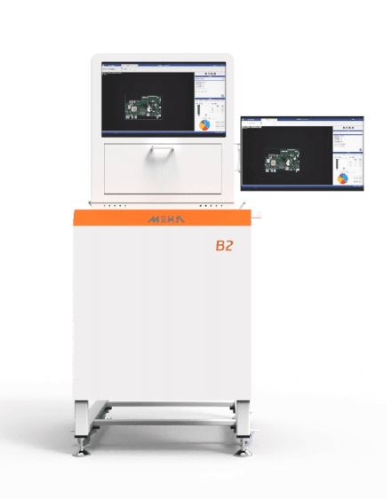
CTW MEKA DIP AOI B2 Before-Wave / B2 Go After-Wave
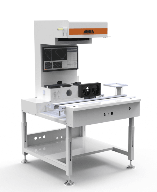
CTW MEKA DIP AOI B2 series includes Before-Wave and After-Wave models for THT DIP PCBA inspection. Detects missing through-hole parts, bent pins, polarity error and wave solder defects for through-hole assembly lines.
CTW MEKA B2 inline DIP AOI is specially developed for THT through-hole assembly production lines. The B2 Before-Wave is deployed before wave soldering, checking inserted components, pin bending, missing parts and reversed polarity before boards enter the wave solder oven. B2 Go After-Wave inspects PCBs after wave soldering to catch solder bridges, insufficient solder, pin holes and soldering defects.
Both models adopt large FOV camera system with planar + 4-side angle lighting, supporting PCB panel up to 1000mm length. Built-in AI programming reduces setup time, ideal for electronics manufacturers with mixed DIP batch production.
Core Advantages
Dedicated for THT DIP Wave Soldering ProcessTwo versions to fit pre-wave and post-wave inspection stages, cover full through-hole assembly quality control.
Large Field of View & Long PCB SupportSupports PCB length up to 1000mm, compatible with panelized DIP boards. 20MP /25MP /65MP optional high resolution camera.
AI One-Click ProgrammingAI component library speeds up new program creation, reduces engineer programming workload. Multi-angle lighting handles tall through-hole components.
Rigid Mechanical Frame & SMEMA CompatibilityStable inline conveyor, standard SMEMA interface to connect with wave solder machine and other DIP line equipment. SPC quality data report function.
Model Comparison Table
| Model | Application Stage | Core Feature |
|---|---|---|
| B2 Before-Wave | Before wave soldering | Check inserted THT components: missing parts, bent pins, reversed polarity, wrong components |
| B2 Go After-Wave | After wave soldering | Inspect wave solder defects: solder bridge, insufficient solder, pin hole, bad solder joint |
Key Specifications
| Item | Parameter |
|---|---|
| Inspection Principle | Multi-angle 2D optical imaging with planar + side LED lighting |
| Detectable Defects | Missing THT component, bent pin, reversed polarity, solder bridge, insufficient solder, pin hole, foreign object |
| Max PCB Length | Up to 1000mm |
| Camera Option | 20MP /25MP /65MP high resolution camera |
| Programming | AI assisted component library + image teaching |
| Communication | SMEMA standard |
| Software Function | Defect classification, SPC statistics, production report, defect traceability |
Machine Details
Multi-angle segmented LED lighting system (plane + four side lights)
Large FOV high resolution industrial camera
Anti-vibration rigid machine frame
Inline automatic PCB conveyor for long DIP panels
Industrial touch screen HMI, AI fast programming
Built-in SPC quality statistical module
SMEMA compatible with DIP wave soldering production line
RELATED PRODUCTS
Inspection & Rework Systems
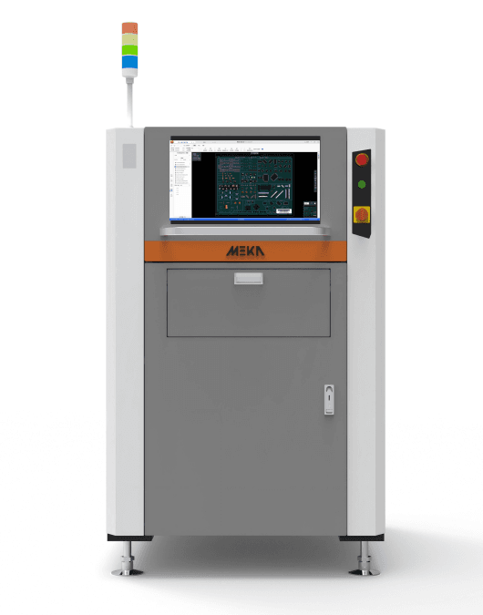
CTW MEKA 2D AOI M2 / M2 Pro / M2 Pro Max
Inspection & Rework Systems
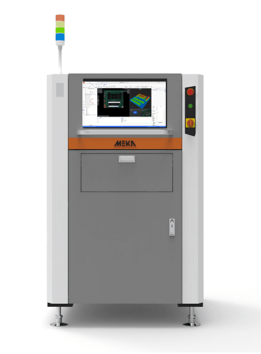
CTW MEKA 3D AOI M3 / M3 Pro / M3 Pro Max / M3 Ultra
Inspection & Rework Systems
CTW MEKA RS PCBA Rework Station
Inspection & Rework Systems